VLSI DESIGN STYLES:

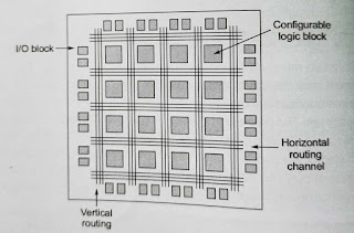
1 FIELD PROGRAMMABLE GATE ARRAY (FPGA) DESIGN: Field programmable gate array( FPGA) is a fully fabricated IC chip in which the interconnections can be programmed to implement different functions. An FPGA chip has thousands of logic gates which are to be connected to be implement any logic function. A typical FPGA architecture is shown in fig. It has the following three main components: 1. 1 . I/O buffers 2. 2. Array of configurable logic blocks(CLBs) 3. 3. Programmable interconnects. Fig:Typical FPGA architecture Picture Source/courtesy: wikipedia In the FPGA- based design ,first a behavioural netlist is written to describe the functionally of the design. This is done using the hardware description languages such as Verilog or VHDL. Then the netlist is synthesized to come up with the gate level design. The next step is to map the logic blocks in to available lpgic cells. This progr...


